Aluminum Nitride Substrate
Aluminum nitride (AlN) is a advanced technical ceramic material that features an extremely interesting combination of very high thermal conductivity(up to230 W/m.K) and excellent electrical insulation properties.
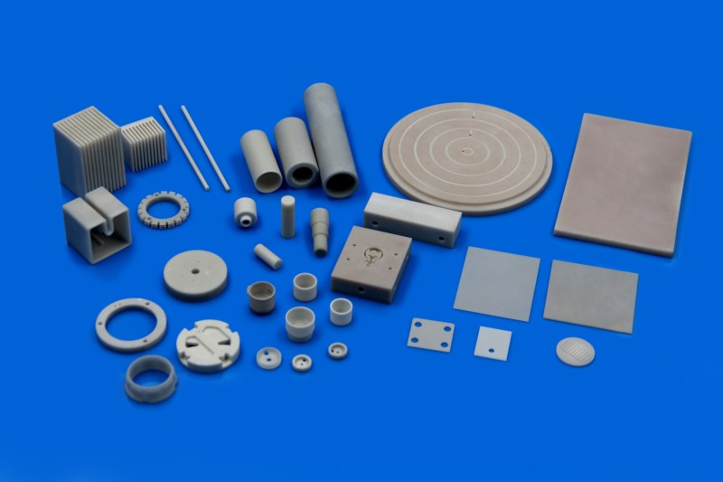
This makes aluminum nitride (AlN) ceramic substrate widely use in power electronics and microelectronics. For example, it is used as a circuit carrier (substrate) in semiconductors or as a heat-sink in LED lighting technology or high-power electronics.
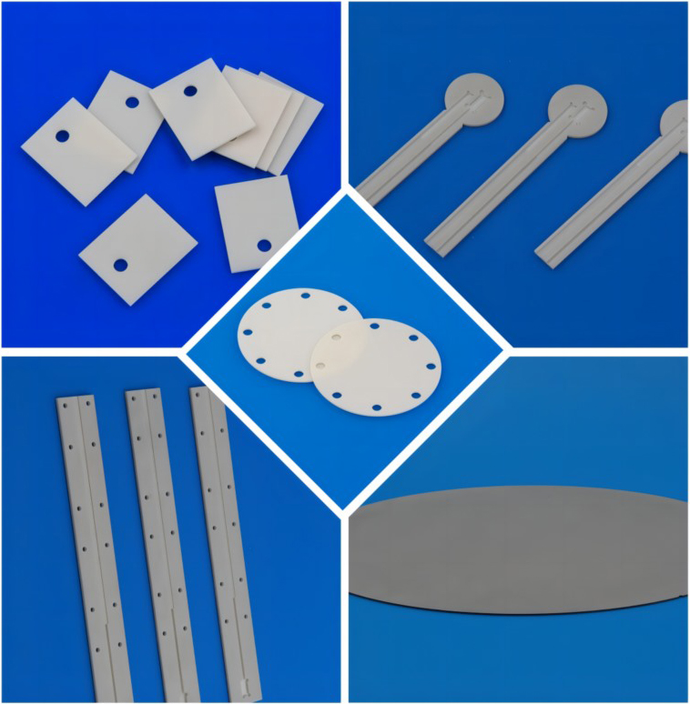
Aluminum Nitride(AlN) Ceramic Substrate Advantages
·High thermal conductivity (170-230W/mK), up to 9.5 times than that of Aluminum Oxide ceramic substrate.
·Similar coefficient of thermal expansion to that of silicon (Si), GaN, and GaAs semiconductors. This helps to achieve high reliability of silicon (Si) chip and thermal heat-up cycling.
·High electrical insulation, and smaller dielectric constant.
·High mechanical strength (450MPa).
·Superior corrosion resistance against molten metal.
·Very high purity, no toxicity.
Material Properties of AlN Ceramics:
| Properties | Unit | AN170 | AN200 | AN230 | AN99 | AN999 |
| Color | – | Gray | Gray | Beige | Gray | Beige |
| Content of AlN | – | ≥95% | ≥95% | ≥96% | ≥99% | ≥99.9% |
| Bulk Density | g/cm3 | ≥3.30 | ≥3.30 | ≥3.28 | ≥3.26 | ≥3.25 |
| Flexural Strength | MPa | ≥400 | ≥300 | ≥300 | ≥300 | ≥300 |
| Compressive Strength | MPa | 2500 | 2000 | 2000 | 2000 | 2000 |
| Hv 500g | Gpa | 10.5 | 9.5 | 9 | 9 | 9 |
| Young’s Modulus | Gpa | 300 | 300 | 300 | 280 | 280 |
| Thermal Conductivity (@20°C) | W/m·K | ≥170 | ≥200 | ≥220 | ~100 | ~90 |
| Specific Heat | KJ/(Kg·K) | 0.74 | 0.74 | 0.73 | 0.73 | 0.73 |
| C.T.E (r.t.-400°C) | 10-6/K | 4.6 | 4.6 | 4.6 | 4.6 | 4.6 |
| Volume Resistivity | Ω·cm 20°C | ≥1014 | ≥1014 | ≥1013 | ≥1010 | ≥1010 |
| Dielectric Strength | KV/mm | ≥16 | ≥16 | ≥15 | ≥15 | ≥15 |
| Dielectric Constant (@1MHz) | – | 8.6 | 8.6 | 8.6 | 8.6 | 8.6 |
| Loss Tangent (@1MHz) | ×10-4 | 5 | 5 | 5 | 5 | 5 |
·Aluminum Nitride(AlN) Ceramic Substrates Applications
·Microelectronics: Ideal for use in integrated circuits and electronic devices.
·LED Packaging: Ensures effective heat management in LED applications.
·Power Electronics: Used in power modules and high-frequency circuits.
·Semiconductor Manufacturing: Provides a stable platform for semiconductor devices.
·Microwave and RF Components: Suitable for applications requiring high-frequency performance.
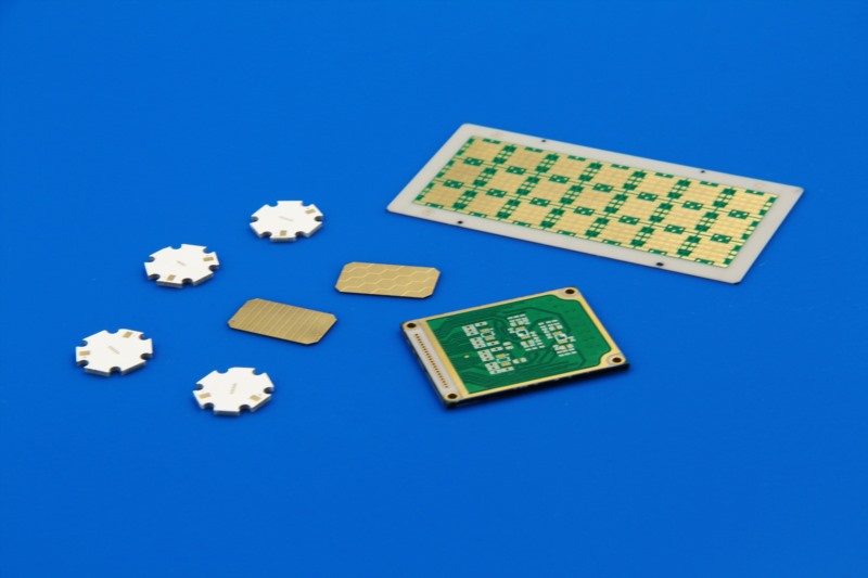
·Aluminum Nitride (AlN) Ceramic Substrates available for various metallization process, like Thin film, Thick film, Direct Bonded Copper, Active Metal Brazing and Direct Plated Copper.
In-House Advanced Machining Processes
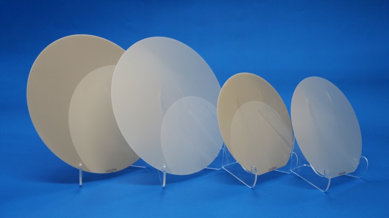
Innovacera provides all the advanced services you need to shorten lead times and improve component quality.
Surface Finishes:
AF = As Fired
LBS = Lapped Both Sides (25u” Ra)
PBS = Polished Both Sides (2u” Ra)
P1S = Polished 1 Side (2u” Ra) / 2nd Side Lapped
Improved tolerances, surface finishes and alternate sizes are also available.
Standard & custom substrate available
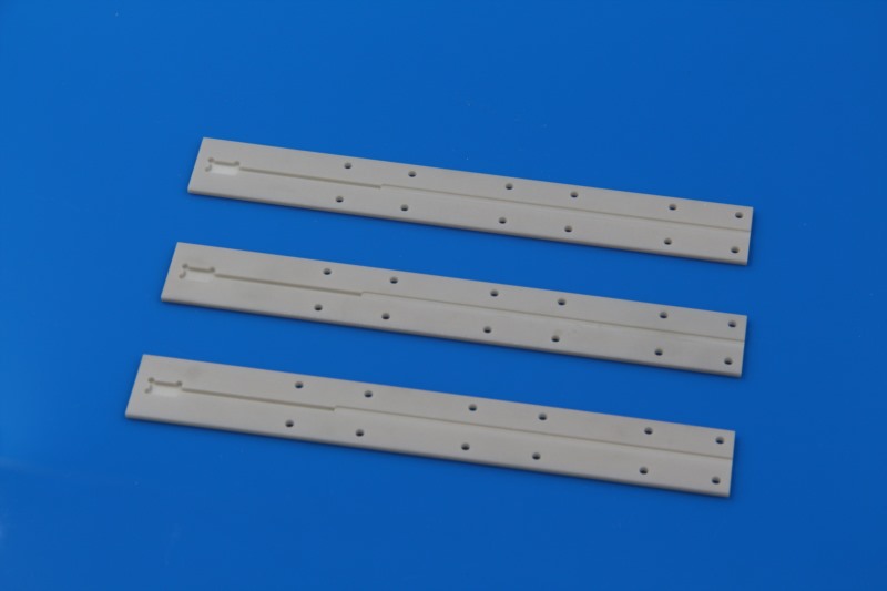
Standard squares: 25.4mm, 50.8mm, 101.6mm and 114.3mm (1ʺ, 2ʺ, 4ʺ, 4.5ʺ)
Standard rounds: Φ101.6mm,Φ152.4mm, Φ203.2mm,Φ304.8mm and Φ356mm (4ʺ, 6ʺ,8ʺ,12ʺ,14ʺ)
Thickness available: 0.2~25.4mm (0.008ʺ to 0.140ʺ)
Custom shapes and sizes available for quoting!
Consult with Innovacera Engineers
Innovacera has a highly qualified staff to assist with material selection and product design. Please contact us today at +86 592 558 9730 or sales@innovacera.com for more information.
Comments
Post a Comment