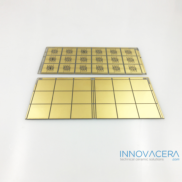
Direct Plated Copper Substrate
Direct Plated Copper (DPC) is a newest development in the field of Ceramic Substrate PCBs, its process is by magnetron sputtering technology to deposit a metal layer (Ti/Cu target) on the surface of the ceramic substrate which result in copper thickness’ ranging from 10um to 130um, and then photolithography to form circuit patterns. electroplating is used to fill in the gaps and thicken the metal circuit layer, and the solderability and oxidation resistance of the substrate is improved through surface treatment, finally remove the dry film and etch the seed layer to complete the substrate.
Direct Plated Copper Substrate Key attributes :
– Superior CTE and excellent thermal conductivity
– High reliability and durability
– Good Mechanically performance
– Low electrical resistance conductor traces
– Superior high-frequency characteristics
– Fine line resolution
– Low temperature process (below 300℃) guarantee the quality of ceramic and the metallized layer, also reduce the cost.
Direct Plated Copper Substrate Applications:
– High Power LED Packaging
– Hybrid and electric automobile power management electronics
– RF microwave communication
– Substrates for solar concentrator cells
– Power semiconductor packaging
– Laser system
– Fiber laser pump
DBC vs DPC
DBC being suited to high current capacity, however limited on circuit design. DPC allowing for finer tracks and through hole connection.

Comments
Post a Comment